Exploring Phosphorene
Exploring Phosphorene
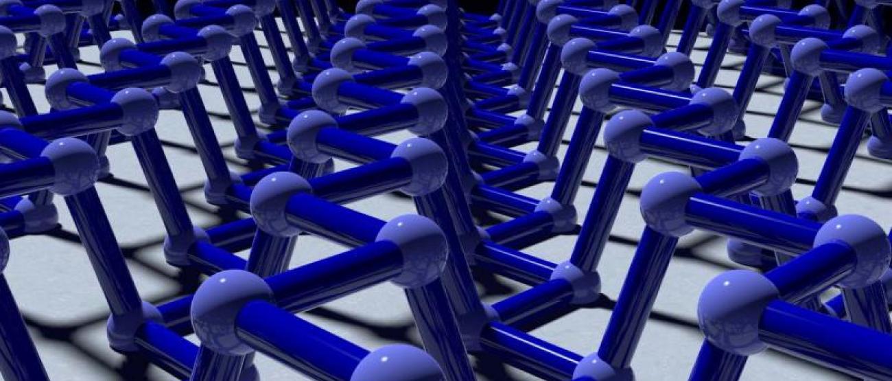
Two-dimensional phosphane, a material known as phosphorene, has potential application as a material for semiconducting transistors in ever faster and more powerful computers. But there’s a hitch. Many of the useful properties of this material, like its ability to conduct electrons, are anisotropic, meaning they vary depending on the orientation of the crystal. Now, a team including researchers at Rensselaer has developed a new method to quickly and accurately determine that orientation using the interactions between light and electrons within phosphorene and other atoms-thick crystals of black phosphorus.
Phosphorene—a single layer of phosphorous atoms—was isolated for the first time in 2014, allowing physicists to begin exploring its properties experimentally and theoretically. Vincent Meunier, head of the Department of Physics, Applied Physics, and Astronomy and a leader of the team that developed the new method, published his first paper on the material—confirming the structure of phosphorene—that same year.
Meunier says Raman spectroscopy uses lasers to deliver energy toward the phosphorene that causes it to vibrate intrinsically. However, lighting the material from different directions would produce varying results because of the electron and light interaction within the material. With this, the electron-photon interaction, in itself, is anisotropic as well.
Meunier and researchers at Rensselaer contributed to the theoretical modeling and prediction of the properties of phosphorene, drawing on the Rensselaer supercomputer, the Center for Computational Innovations, to perform calculations. Meunier and his team are able to develop the potential of new materials such as phosphorene to serve in future generations of computers and other devices.